 MB Manufacturing's pallet is featured on the cover page of Circuits Assembly, January 2009 addition. Follow the link to the on-line magizine. The featured article is on page 26, "Wave Pallet Design Moves Ahead."
Issue: http://www.circuitsassembly.com/cms/magazine/202/7668-january-2009-issue
Selective Wave Soldering DoE to Develop DfM Guidelines for Lead and Pb-Free Assemblies
Written by Makram Boulos, Craig Hamilton, Mario Moreno, Ramon Mendez, German Soto and Jessica Herrera
Wednesday, 31 December 2008 19:00
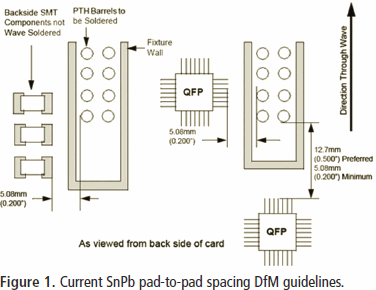
The minimum PTH-to-SMT pad-to-pad spacing for SAC 305 cannot be less than 0.250" without a significant rise in barrel-fill defects.
A number of design guidelines have been used for years to support and optimize SnPb solder use. Most SnPb guidelines were established through experimentation, some directly through experience. Many companies and consortia have defined small variations to central design specifications to help accommodate specific needs. However, most are “flavors” of the widely accepted general guideline. For Pb-free alloys, there is little information to support the validity of current SnPb guidelines defined and, moreover, there is the question of whether the same guidelines would apply to all the various types of Pb-free alloys on the market today.
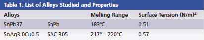
Double-sided assemblies with through-hole technology can either be soldered using a selective solder, point-to-point soldering machine, or by using the wave soldering machine in conjunction with product-specific selective wave pallets. As the pallet opening size correlates to solder’s ability to flow and adequately fill PTH barrels, design guidelines recommend the minimum bottom-side P2P spacing for bottom-side SMT components adjacent to PTH barrels (Figure 1). In this case, the recommendation is a minimum 0.200" (copper-to-copper) gap between the edge of the nearest SMT component pad and the PTH barrels. For Pb-free alloys, this spacing recommendation was increased to 0.250" because the fluidity of Pb-free alloys is less than that of SnPb. Using a designed experiment, this article will confirm these recommendations for both SnPb and a Pb-free alloy (SAC 305) (Table 1).
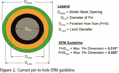
In addition, other DfM aspects will be studied, such as the effect of pin-to-hole ratio on barrel fill, for SnPb and SAC 305 alloys. Because of a lack of historical data, there is a specific interest in assessing the validity of the current pin-to-hole ratio guidelines for Pb-free solders. Current guidelines for SnPb recommend a minimum spacing of 0.015" and a maximum spacing of 0.020" (Figure 2). Finally, the impact of the number of ground layer connections and thermal relief style will be discussed.
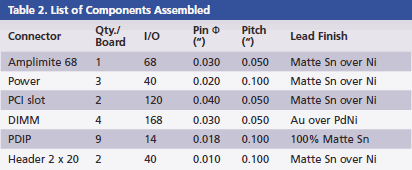
The test vehicle used for this study (Table 2) was designed to represent a mid-level complexity PCB. The dimensions are 8" x 10", with a thickness of 0.093". It consists of a total of 12 layers, with four two oz.-ground layers. It has an OSP surface finish (to represent the most difficult soldering conditions) and a high Tg FR-4 laminate, suitable for Pb-free wave solder processing.
Experimental Methodology
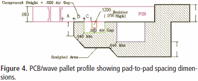
Selective pallet DoE. To determine the minimum distance at which a bottom-side SMT component can be placed from a PTH location, a DoE was established, which required the design of five different selective pallets (using 6 mm composite material). Each pallet would provide varying levels of spacing, between the outside copper edge of the barrel and outside copper edge of an SMT pad (see “A+D+C” in Figure 4).
The five different spacing distances were achieved by designing five unique fixtures with different opening sizes that correlated to five spacing patterns selected. The five spacing designs were 0.250" (current recommended spacing for Pb-free), 0.200" (current recommended spacing for SnPb), 0.150", 0.100" and 0.050" (Table 3). A total of 25 boards were assembled per alloy, five boards per spacing level. All barrels inspected were designed with “standard” features (e.g., standard pin-to-hole ratios and thermal relief, four-spoke design). Barrel fill was inspected using IPC-A-610 Class 2 specifications, and DPMO levels calculated.
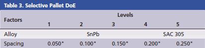
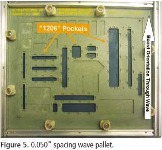
Selective pallet design. Pallet designs were based on manufacturer’s recommendations for minimum wall thickness. The goal was to determine the minimum achievable spacing (i.e., gap between pallet wall and PTH copper edge) without the need for inserts; hence, pallets were designed without the use of titanium inserts. Titanium inserts do permit tighter spacing; however, they correlate to higher manufacturing cost. To maintain pre-established pad-to-pad spacing for the 0.050" and 0.100" spacing, it was necessary to reduce the wall thickness to 0.030" and 0.050", respectively. A wall thickness of 0.050" was the minimum thickness recommended by the pallet supplier. The 0.030" wall thickness, although possible to fabricate, had a higher probability of damage and was not guaranteed to sustain long-life use, especially on longer pallet seal walls. Figure 5 shows one of the fabricated fixtures and the wave solder orientation. The key feature within all the designs was pallet opening size. The TV itself was not designed with tightly spaced SMT components next to PTH barrels, as this was not a requirement for this experiment. However, to simulate and validate the fabrication process, the pallet design included various milled out pockets surrounding each of the openings. The pocket design features (i.e., pocket depth, wall thickness) were based on simulating the presence of 1206 resistors or capacitors.
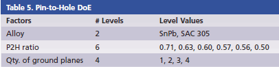
Pin-to-hole (P2H) ratio design. To study the impact of pin-to-hole ratio on barrel fill, a DfM pattern was designed into the TV. A total of six different hole sizes were incorporated onto the power connector location (Figure 6). The connector pin diameter was a constant 0.020" ± 0.005".
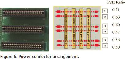
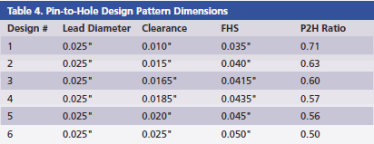
Each row of the three dual-row power connectors had a different finished hole size. This provided six different P2H ratios (Table 4). Based on the maximum dimension of the pin (0.025") and current DfM guidelines, the recommended P2H ratios fell between 0.63 and 0.56. Therefore, a slightly greater and a reduced clearance were tested. In addition to varying the P2H ratio along this connector, each pin also incorporated differing ground layer connections, ranging from zero to four ground layers. The final DoE followed for this study is illustrated in Table 5.
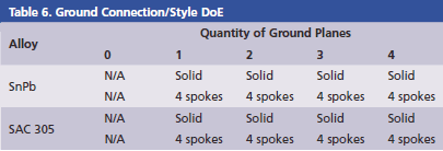
Ground connection and thermal relief design. Four DIMM connectors were used in the test vehicle to study the performance of two different PTH connection types (solid and four-spoke), ranging from one to four ground layer connections (Figure 7). The DIMM connectors ran parallel to the wave solder as a worst-case scenario. Barrel fill analysis was performed using 3-D x-ray to compare performance of the SnPb vs. SAC 305 alloys based on the quantity of ground planes and PTH connection type combinations. The DoE is illustrated in Table 6.
Experimental Procedure
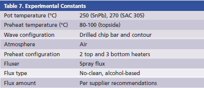
Machine and profile parameters. A standard dual waved solder machine was used throughout this experiment. Wave and flux setup was performed using a temperature profiler, Wave Optimizer and Flux-O-Meter. In addition, a total of 10 boards were used prior to the DoE build to further optimize the profile for both the SnPb and SAC 305 alloys. The parameters, maintained as constants throughout, are in Table 7.
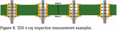
Inspection strategy. All boards were x-rayed using a 5DX laminographic x-ray inspection system to measure the barrel fill of each PTH barrel. All barrel-fill-related defects were inspected based on IPC-A-610, and IPC-79123 was followed to calculate DPMO levels. A five-slice inspection program (Figure 8) was created to measure each of the barrels at slices equivalent to 0% (Slice 1), 25% (Slice 2), 50% (Slice 3), 75% (Slice 4) and 100% (Slice 5). The statistical analysis was based on Class 2 specifications for barrel fill. However, a DPMO comparison between using a Class 2 vs. Class 3 specification level was also performed.
Results and Discussion
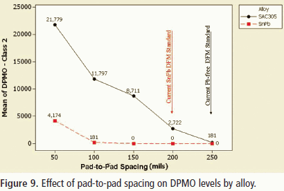
Selective pallet DoE. The results of the DoE were plotted in terms of average DPMO levels based on Class 2 barrel-fill inspection criteria (Figure 9). This illustrates the impact of both pad-to-pad spacing (i.e., pallet opening) and alloy (SnPb vs. SAC 305). The figure also highlights the current SnPb and Pb-free DfM guideline standards for P2P spacing of 0.200" and 0.250" respectively. The first observation, as expected, illustrates the improved barrel-fill performance of the SnPb alloy, having statistically superior results compared to SAC 305, at all levels of P2P spacing. It can be seen, based on these results, that the SnPb spacing of 0.200" provides a conservative degree of spacing, with possible room for further reducing the specification to as low as 0.150" without impacting yield. With respect to the Pb-free results, the change in defect levels between all levels of P2P spacing is dramatic in overall barrel-fill yields. The data also show that 0.250" spacing is absolutely required when using SAC 305 alloy and further spacing (greater than 0.250") recommended when possible.
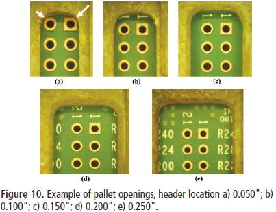
A visual illustration of the actual spacing levels is shown in Figure 10a-e. It can be seen that the 0.050" P2P spacing surrounding the 2 x 20 pin header location provides very little clearance between the pallet wall and the PTH annular ring (especially at the corner locations). The corner radius was the smallest possible radius the pallet supplier could achieve. It is clear to see how soldering the PTH locations with a pallet opening required to shield a 0.050" P2P spacing would be very difficult.
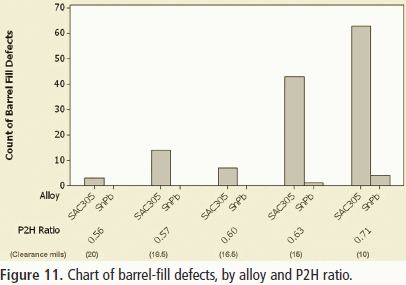
Effect of P2H ratio. The results of this experiment (Figure 11) show the Class 2 barrel fill defects by alloy and P2H ratio. The results indicate that barrel fill improved with 1) alloy type and 2) decreasing P2H ratio (i.e., increasing hole clearance). The results suggest potential to increase the current SnPb P2H ratio design guidelines. Where possible, however, it is recommended to incorporate smaller P2H ratios (i.e., larger hole clearance) to assist in barrel fill, especially in Pb-free applications.
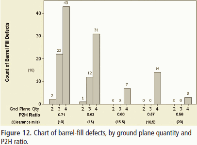
Further analysis showed 73% of the combined SnPb and SAC 305 barrel-fill-related defects occurred on pin locations attached to four-layer, thermal relief grounds (Figure 12). Looking specifically at defects occurring between the current DfM P2H guidelines (0.56 – 0.63), those pins attached to three layers or fewer accounted for 20% of the total defects, with four ground layers having the most significant impact. Hence, there is a significant impact of both the number of ground connections and the P2H ratio on barrel fill defects.
Effect of ground connection and thermal relief. It was shown that the number of ground layers has a significant effect on the level of barrel fill achieved. This section shows the interaction between the number of ground layers and P2P spacing. It also illustrates the impact of solid ground connections vs. a thermal relief four-spoke design. Based on the analysis, it can be seen that both the number of ground layers and thermal relief design have a significant impact on the barrel-fill results achieved.
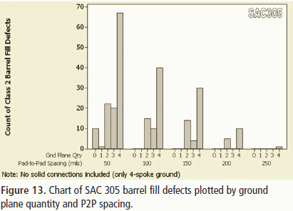
Figure 13 illustrates the interaction between the quantity of ground connections (four-spoke only) and P2P spacing on barrel fill, using SAC 305. These results again illustrate the significant impact the number of ground layers, in addition to the effect a smaller pallet opening, has on barrel-fill defects.
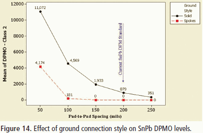
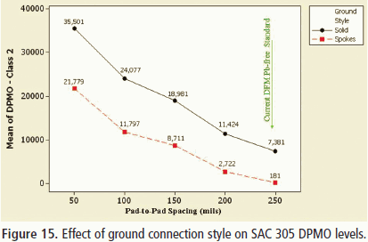
Figures 14 and 15 show the impact ground connection style has when using SnPb and SAC 305, respectively. In both cases, regardless of alloy, the impact of using a solid ground connection (i.e., no thermal relief) is extremely significant. When considering a solid ground connection, DPMO levels increase from zero (spokes) to 879 (solid) DPMO, when using the current SnPb P2P spacing limit of 0.200" (Figure 14). The results when using SAC 305 are further amplified, with the DPMO levels increasing from 181 (spokes) to 7381 (solid) DPMO at the current Pb-free P2P spacing limit of 0.250" (Figure 15).
Here is a summary of the overall statistics based on the following total barrel-fill (BF) defect results:
SnPb = 107 defects & SAC 305 = 554 defects.
Ground Connection
SnPb: 90% of BF defects attributed to having a ground connection.
SAC 305: 98% of BF defects attributed to having a ground connection.
Number of Ground Layers (0-4 ground layers)
SnPb: 84% of BF defects attached to 4 layers.
SAC 305: 73% of BF defects attached to 4 layers.
Ground Connection Style (none, 4 spoke & solid)
SnPb: 78% of BF defects attributed to a solid ground connection.
SAC 305: 55% of BF defects attributed to a solid ground connection.
SAC 305: 43% of BF defects attributed to a 4-spoke ground connection.
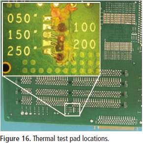
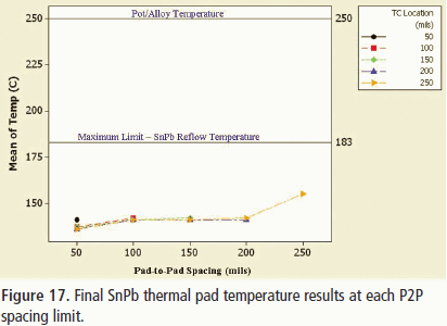
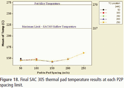
Temperature shielding effectiveness. A frequent question when using a selective wave solder pallet is how well the pallet material acts in shielding the covered SMT components from the high alloy temperatures during soldering, especially when converting to Pb-free temperatures. To answer this, a series of thermal pads were designed into the test vehicle, adjacent to a DIMM connector location. The test pads were designed at 0.050" - 0.250" from the edge of the outer row of DIMM barrel leads (Figure 16). Thermocouples were drilled from the topside and soldered onto the thermal pads located on the bottom-side. The dimensions of the thermal pads represented an adjacent 1206 component pad.
Temperatures were monitored during assembly of both a SnPb and SAC 305 board, using all five selective pallet designs (Table 7). All the thermocouple locations were monitored during the assembly. Therefore, some of the test points were exposed to solder (i.e., those not shielded) during wave soldering. Those test points directly exposed to solder (i.e., empty cells in Table 7), were not included in the following analysis. When plotting the results of the SnPb and SAC 305 builds, it can be seen that the pallet material was able to limit the temperature of the shielded test pads to well below the reflow temperature of both the SnPb (Figure 17) and Pb-free (Figure 18) alloys, hence providing adequate shielding to avoid any occurrences of secondary reflow during the wave soldering process. This applied for all pallet designs, even with the smaller pallet wall thickness (0.030") associated with the 0.050" design.
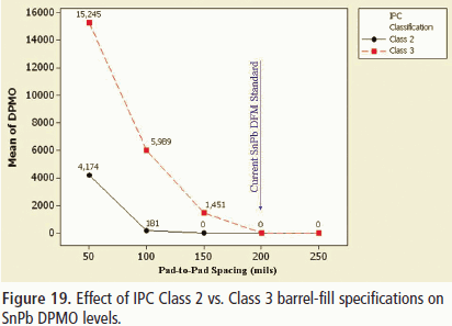
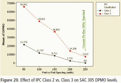
Effect of Class 3 specification. Another observation that resulted from this work was the impact of IPC classifications of barrel-fill defects on the overall DPMO levels. The SnPb results (Figure 19) at the current P2P spacing limit of 0.200" show no change in DPMO levels when inspecting to either a Class 2 or Class 3 specification. However, as the P2P spacing limit is reduced to 0.150" and below, the DPMO levels increase significantly when inspecting to 75% overall barrel fill (i.e., Class 3). This shows the majority of defects occurring were at pin locations connected to ground, which, if >50% filled, would have passed Class 2. When converting to Pb-free, the results are exacerbated with a 40X increase in DPMO at the current 0.250" spacing, and an exponential increase of DPMO levels at the decreased levels of P2P spacing (Figure 20). These results indicate significant increases in DPMO levels when inspecting to 75% barrel fill (i.e., Class 3). Changes to P2P spacing now become difficult when using Class 3 specifications.
Conclusion
The main outcome of this work proves the limitations of SAC 305 alloy in achieving comparable levels of barrel-fill yield compared to SnPb alloy. The results from this experiment show the minimum PTH-to-SMT pad-to-pad spacing when using SnPb alloy may be reduced to 0.150" without causing a significant increase in barrel-fill deficiencies. Maintaining as large an opening as possible when using selective pallets to improve barrel fill is recommended, however. The results show the minimum PTH-to-SMT pad-to-pad spacing when using SAC 305 alloy cannot be less than 0.250" without causing a significant increase in barrel-fill defects. Barrel-fill defects increased to 181 DPMO (from zero defects using SnPb) at the 0.250" pallet opening. It is recommended to maintain the current DfM standard for pad-to-pad spacing for Pb-free at 0.250". Note: These conclusions were drawn when inspecting to Class 2 barrel-fill specifications.
The results also showed DPMO levels increased with an increasing P2H ratio (i.e., smaller hole clearance). The results suggest there may be capability in increasing the current SnPb P2H ratio DfM design guidelines. However, it is recommended, where possible, to incorporate smaller P2H ratios (i.e. larger clearance) to assist in barrel fill, especially in Pb-free applications. This finding was similar to other published results on P2H ratio.4,5 In addition, those barrels attached to ground, and especially those using a solid ground connection, had the largest influence on DPMO levels. The results showed that incorporating thermal relief (i.e., four-spokes) into the ground layer design helped improve barrel fill compared to having a direct solid connection. A solid ground connection had a major impact on DPMO levels, regardless of alloy used, and should be avoided wherever possible.
In this specific experiment when using selective pallets, it can be seen DPMO levels increased significantly between using Class 2 & Class 3 IPC inspection criteria. In this case, the majority of defects occurring resulting from Class 2 specifications were grounded pins with less than 50% vertical fill. The results of this experiment showed the impact on DPMO when converting from SnPb to Pb-free, regardless of the class (2 or 3) of inspection criteria. When using Class 2 criteria with standard features, the DPMO increased from zero to 181 when converting from SnPb to SAC 305. Using Class 3 criteria with standard features, the DPMO increased from zero to 7,623 when converting from SnPb to SAC 305. With the impracticality of further increasing the P2P spacing limits (i.e. > 0.250") for Pb-free, and considering a lack of impact on ground connection designs, the impact of using the current Class 3 IPC specification on DPMO levels is significant. Efforts in reducing IPC Class 3 specification limits, provided the reliability requirements can be met, would assist in minimizing these impacts to wave solder yields, and potentially allow tighter SMT to PTH spacing. This is especially important when considering thicker card assemblies.
Future Work
Based on the expected difficulty in being able to satisfy current IPC Class 3 barrel-fill requirements when soldering large thermally massive PCBs (currently under RoHS exemption), further study into the impact of % barrel fill on PTH solder joint reliability will be performed. This will be correlated to other industry studies published on this topic.6 In addition, future work will study process limitations of wave soldering high complexity/mass PCBs, when using a selective wave solder process and SAC 405 alloy. Further comparisons between SAC 305 and SAC 405 with regard to barrel fill will be measured based on earlier work.7 In addition, recent wave solder machine wave form developments might also help improve hole fill and need to be verified as to their effectiveness on thicker, more thermally challenging assemblies.
Acknowledgments
This paper is dedicated to the memory of Makram (Mike) Boulos. He will be remembered for his constant quest for knowledge, desire for change and impact to the industry.
The authors would like to extend our appreciation and acknowledge the organizational support of both Honeywell and Celestica that enabled this study. The consultation provided by Jeffrey Kennedy of Celestica was particularly helpful. Thank you to Elaine Hui of Celestica for assistance with pallet design and to the Celestica design team: Denesh Ramsamujh and Malcolm Simpson.
References
- IPC-A-610D, Acceptability of Electronic Assemblies, February 2005.
- B. Huang, A. Dasgupta and N-C. Lee, “Effect of SnAgCu Composition on Reflow Behavior,”Amsterdam, 2004.
- IPC-7912, Calculation of DPMO and Manufacturing Indices for Printed Board Assemblies, July 2000.
- R. Mendez, C. Hamilton, “Design for Manufacturability in the Lead Free Wave Solder Process,” IPC Apex, April 2008.
- J. Nguyen, et al, “Impact of Hole-Fill and Voiding on Pin Through-Hole Solder Joint Reliability,” Apex, April 2008.
- H. Holder, et al, “Reliability of Partially Filled SAC 305 Through-Hole Joints,” IPC Apex, February 2006.
- C. Hamilton and M. Kelly, “A Study of Alternative Lead Free Wave Alloys: From Process Yield to Reliability,” IPC Apex, April 2008.
The late Makram (Mike) Boulos was with Honeywell Aerospace (honeywell.com). Craig Hamilton, Mario Moreno, Ramon Mendez, German Soto and Jessica Herrera are with Celestica (celestica.com)